top of page
PRODUCT DIRECTORY

2Dx® Masterbatch
2D fab
Our 2Dx® Masterbatch has shown a 30–50% increase in stiffness with concentrations as low as 0.5–1.5wt% graphene, enabling the construction of stronger products and more lightweight redesigns.
Additionally, enhancing polycarbonate with graphene improves:
- Impact resistance
- Heat conductivity
- Electrical conductivity
- Flame resistance

Park FX40
Park Systems
Park FX40 transforms atomic force microscopy, placing user benefits at the forefront through groundbreaking autonomy and advanced technology. Integrated intelligence and robotics automate set up and scanning tasks, freeing researchers from manual operations. This includes managing probes, alignment, sample positioning, and imaging optimization, allowing users to focus on their specialized work. With improved electromechanics, noise reduction, and multi-sample imaging, the FX40 streamlines data collection, research workflows, and data publication, empowering accelerated scientific progress and discovery.

NanoCuvette™ S
Copenhagen Nanosystems (cphnano)
The NanoCuvette™ S from @cphnano allows for spectrophotometric quantification of particle/cell size and concentration analysis in numerous industries and research fields such as biotechnology, pharmaceuticals, life science, foods, including various industrial applications for quality control.
The capacity of NanoCuvette™ S goes far beyond any product currently on the market in terms of achieving easy, affordable, and reliable particle/cell size analysis and concentration determination. With the NanoCuvette™ S you have the functionality to determine small particles down to 50 nm, while simultaneously quantifying their concentration using your existing UV-Vis spectrophotometer.
Learn more: https://shop.cphnano.com/products/nanocuvette-s
15% discount using promo code "NWA2024".
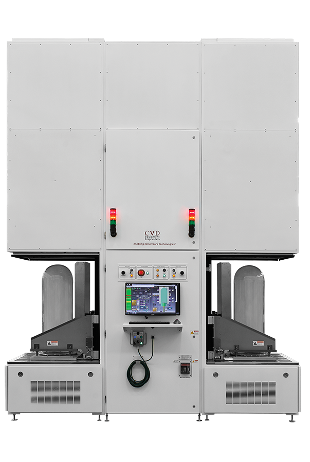
Chemical Vapor Infiltration (CVI) Systems
CVD Equipment Corporation
Chemical vapor infiltration (CVI) is a chemical vapor deposition (CVD) process that is performed at low pressures to allow for coating the internal surfaces of a porous material. Using heat and low pressure, precursor vapors penetrate the pores / fibers of the material and deposit to form a conformal coating on the internal surfaces.
Our CVI platform is used to coat the internal surfaces of porous materials having complex shapes and geometries. Multiple systems are in production for coating biocompatible porous material used in medical implants and aerospace components.
chemical Vapor Infiltration
Park NX-Hivac

Park Systems
Park NX-Hivac is a high vacuum AFM ideal for precise semiconductor failure analysis and sensitive materials research. Operating in a high vacuum environment, it delivers enhanced accuracy and repeatability, minimizing tip and sample damage. It's the key to a range of applications, including dopant concentration assessment using Scanning Spreading Resistance Microscopy (SSRM). With Park Systems’s intuitive Hivac Manager and automatic vacuum control, Park NX-Hivac streamlines the vacuum process and offers rapid vacuum conditions. Park NX-Hivac offers high-precision research in an oxygen-free vacuum environment.
Atomic Force Microscopy (AFM), High Vacuum Environment
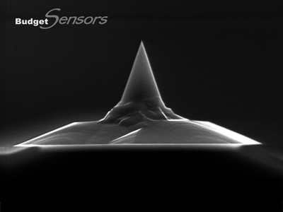
Tap190Al-G
BudgetSensors
Monolithic silicon AFM probe for high frequency non-contact and tapping mode operation.
The rotated tip allows for more symmetric representation of high sample features. The consistent tip radius ensures good resolution and reproducibility.
The AFM holder chip fits most commercial AFM systems as it is industry standard size. It is compatible with:
Bruker / Veeco / Digital Instruments
Keysight / Agilent / Molecular Imaging
Asylum Research
Park Systems
JEOL
JPK
etc.
BudgetSensors' Tap190-G features a longer cantilever and it is meant as an alternative to BudgetSensors' Tap300 probes series, when the feedback loop of the AFM system does not accept high frequencies (400 kHz) or when the detection system needs a minimum cantilever length > 125 µm. The scanning speed of Tap190 series AFM probes is slightly slower than the scanning speed of the Tap300 series.
For measurements in liquids please use the back side gold coated Tap190GD-G or the overall gold coated Tap190GB-G!
AFM Probe
IR5 FTIR Spectrometer

Edinburgh Instruments
The IR5 is a high-performance benchtop Fourier Transform Infrared (FTIR) spectrometer from Edinburgh Instruments.
The IR5 is the perfect choice for analytical and research applications such as polymer, semiconductor, and pharmaceutical samples, offering simple operation as well as fast and accurate results. IR absorption, transmission, reflectance, and infrared photoluminescence can all be measured in the IR5 using only one software package, Miracle™.
Outstanding Performance – High sensitivity and spectral resolution
Photoluminescence Upgrade – Fourier Transform PL upgrade with a choice of laser source
Configurable – Option for a second detector enhancing sensitivity at selected spectral ranges
User-friendly – Simple to operate and suitable for all user levels, from beginner to advanced
Maintenance Free – No maintenance required with moisture control technology
Miracle™ Software – Powerful and intuitive software designed specifically for the IR5
Instrument, measurement, analysis
Quantum Dots

Creative Diagnostics
Creative Diagnostics provides a comprehensive list of DiagNano™ semiconductor quantum dots with different chemical compositions and surface functionalization. Our quantum dots have uniform size, tunable emission and high quantum yield, as well as good thermal stability. The electronic characteristics and band gap of quantum dots are closely related to its size and shape. By changing the size of our quantum dots, the color of emitted light shifts from blue to near-infrared, which allows the excitation and emission of quantum dots to be highly adjustable, and brings lots of applications for highly sensitive cellular imaging, photovoltaic devices, solar cells, and light emitting devices.
Quantum Dots
NanoDCAL+

Nanoacademic Technologies Inc.
NanoDCAL+ (Nano DFT CALculator plus) is an LCAO implementation of NEGF-DFT.
It is a general-purpose tool for ab initio modeling of non-equilibrium quantum transport. It inherits from NanoDCAL which has been used in hundreds of scientific publications in domains as varied as molecular electronics, nanotubes, topological insulators, batteries, magnetic tunnel junctions, metal grain boundaries and more. Its complementary set of features makes the best technological base for your R&D projects.
Benefits of NanoDCAL+:
Predict the electronic structure of virtually any material.
NanoDCAL+ computes the properties of a given atomic arrangement (molecules, crystals, surfaces, etc.) from first principles using density functional theory (DFT).
Accurately predict non-equilibrium properties of heterojunctions and devices.
NanoDCAL+ derives a device’s Hamiltonian from first principles and accounts for non-equilibrium quantum statistics using Keldysh’s Green function formalism (NEGF) to achieve a description beyond the predictive power of semiclassical transport methods.
Get the answer faster using NanoDCAL+’s powerful implementation.
NanoDCAL+’s high-performance solvers and massively parallel implementation yield the answer faster and allow simulating systems larger and more realistic than ever.
Using NanoDCAL+ is convenient and easy.
You may use NanoDCAL+ from Device Studio to create and visualize materials and devices, or the Python scripting environment which is convenient to automate jobs and workflows.
Key Features:
- Fast & parallel solver
NanoDCAL+ is carefully optimized to get you the answer faster. The code is parallelized using MPI and scales to 1,000’s of cores.
- Transistor simulator
Simulate realistic devices accounting for the effect of gates and dielectric materials consistently.
- IV characteristic
Compute the current versus voltage characteristic to predict nanoscale device performance.
- Transmission & conductance
Get transmission channels and coefficients, conductance for bulk materials, surfaces and devices.
- Python integration
NanoDCAL+ has a friendly Python interface, allowing one to quickly and easily build workflows and visualize data. Choose from our pool of calculators to compute ground state densities, band structures, Hamiltonians, IV curves and more.
- Ground state properties
Predict ground state properties like total energy, atomic forces, stress tensor.
- Spin
Include the physics of electronic spin and spin-orbit coupling via a state-of-the-art spin-DFT implementation (collinear and non-collinear formalisms).
- Atomic orbitals and pseudopotentials
Benefit from our accurate, efficient and complete database of atomic orbitals and pseudopotentials.
software, Simulation
Semiconductor Crystal Growth System
CVD Equipment Corporation
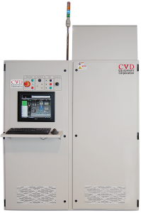
Our Vertical Bridgman Crystal Growth system is an advanced process tool for the growth of bulk single crystal ingots. The system is optimized for controlled process development and user safety.
The Vertical Bridgman Crystal Growth system includes two independently controlled furnace subsystems; the melting and growth furnaces. A linear drive mechanism provides automated precision movement of the furnace assembly through the process zones between a start position and stop position at a programmable velocity profile with minimal vibration.
A high slew-rate mode permits quick setup and removal of the crystal growth crucible or ampoule. A rotary drive subsystem rotates the crucible or ampoule during the process to improve thermal uniformity.
Bulk single crystals, including:
Cd1-XZnXTe | CdSe | CdTe | Mg | ZnS | ZnSe | ZnSe:Cr | ZnTe | Zn1-XMgXSe | Zn1-XMgXSe:Cr
Semiconductor Crystal Growth System
Antimicrobial

S3nano
Our antimicrobial solution can be incorporated into different materials, guaranteeing permanent, high-efficiency protection.
Eliminates up to 99.9% of microorganisms proven by the main standards.
Elimination of more than 650 types of pathogenic bacteria and fungi.
High efficiency in combating gram negative and gram positive bacteria.
Our technology
Permanent antimicrobial protection on the surface and controlled release upon contact;
Effective on the surface and polymer matrix, even after washing or wearing the product;
Protects against cross-contamination.
additives, antiviral, antibacterial, polymers
SR200 Series - Boxcar averager systems

Stanford Research Systems
The SR200 Series Boxcar Averager System is a modular instrumentation platform designed to acquire and analyze fast analog signals. The system consists of a NIM compatible mainframe and modules which can be selected to tailor a system to individual requirements. The SR200 series is flexible enough to handle gate widths from 100 ps to 150 µs, repetition rates up to 50 kHz, and has both analog and digital outputs.
Scientific Instruments
Carbon Nanotubes, Multiwall, Hollow Structure - PD30L5-20

NanoLab, Inc.
You have choosen multiwall carbon nanotubes, hollow structure.Purity > 95%, residuals may include iron, sulfur.OD 30 +/- 15 nmLength 5-20 micronsSSA 200 - 400 m2/gPricing1g: $1105g: $50025g: $2,25050g: $4,500100g: $9,000
Nanomaterial, Raw material
NanoCuvette™ One

Copenhagen Nanosystems (cphnano)
The NanoCuvette™ One is an excellent improvement in any laboratory workflow for quantitative analysis in numerous industries such as biotechnology, pharmaceuticals, chemistry, foods and industrial applications for quality control.
The capacity of NanoCuvette™ One goes far beyond any product currently on the market in terms of concentration determination. With the NanoCuvette™ One you are able to analyze smaller samples (down to 0.5 μL) and a large range of concentrations (0.02 - 300 mg/mL) of non-absorbing compounds.
spectroscopy
Coating Thickness Measurement

Anton Paar GmbH
The Calotest instruments from Anton Paar provide quick, simple and inexpensive determination of coating thicknesses. Employing the simple ball-cratering method, the thickness of any kind of single or multi-layered coating stack is accurately checked in a short time, in full compliance with relevant international standards.
Instrument, measurement, analysis
IBF-700
NTG Neue Technologien
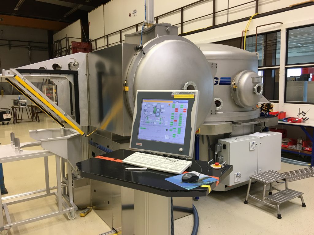
Ion Beam Figuring plant IBF-700The IBF-700 plant is the biggest plant of NTG?s IBF-plant family. Workpieces with a diameter up to 700mm and up to a weight of 70kg can be processed.Loading and unloading also is done via a load lock chamber. That means a continously process is guaranteed.Manually loading is prohibited for workpieces of this size and weight. Therefore the IBF-700 can be equipped with a lifting and turning device or a robot.Ion beam Figuring plant IBF-700Ion beam Figuring plant IBF-700
Instrument, measurement, analysis
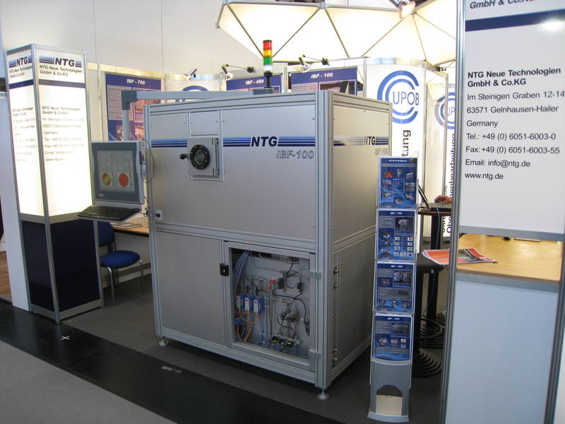
IBF-100
NTG Neue Technologien
Ion Beam Figuring plant IBF-100The Ion Beam Figuring Plant - IBF 100 - is a procedural plant for nanometer exact correction of small surfaces. It is the latest development of NTG. The IBF-100 is a consistent advancement of our bigger plants IBF-300, IBF-450 and IBF-700. The last mentioned plants are sold with great success for nearly 20 years. They are used in the high-end-processing of predominantly large shaped optical parts (PV-value Parts with a diameter of 5-70mm, a max. part thickness of 45mm and a max. angle of 60� can be treated. The components can be onvex, plane or concave. In principle there are nearly any restrictions for the treatment of geometries within the afore mentioned dimensions.This process is realized by a four-axes motion system with one rotary and three linear axes, operating in a vacuum chamber. In the standard procedure the pathway of the Ion Beam spot on the surfaces follows a spherical bowed meander along the lines of latitude. The path velocity on the work surface results from a dwell time distribution proprtional to the desired material removal depth distribution. It is also possible to treat only partial ranges of the surface.NTG uses an inhouse developed control technique for this plant. Control is done via touch screen. The process flow is nearly completely automated. This means for the user: insert work piece, load the program, start the process. All the operating cycles of the plant are documented in a log-file. If requested NTG is able to read the log-file via internet and thus can carry out a remote diagnosis of the plant.Technical Datas:Plant, completeDimensions:length: 1560mmwidth: 1300mmheight: 2170mm, incl. superstructural partsrequired spaceArea: diameter 4m or 3x3mweight: 1.100kgData of the workpiece:max. diameter: 70mmmax. thickness: 45mm incl. support, respectively holderIBF-100 - View Load lock chamberIBF-100 - View revision doorsIBF-100 - Top viewIBF-100 - Laser World of Photonics 2009IBF-100 - Laser World of Photonics 2009
Instruments, Ion Beam Processing
bottom of page

