


Physicists discover ultrafast charge separation in 2D heterostructure
- Mateo Cardinal
- Feb 12
- 10 min read
Monolayer WS₂ on a graphene support for ultrafast separation of charges was studied in a recent article in Nano Letters by a team from University of Regensburg, Universität Bremen, Istituto Italiano di Tecnologia and the University of Hamburg. "Time-Resolved Photoemission Spectroscopy in Angle Mode (trARPES) was used to probe the transient band structure of a two-dimensional heterostructure." They observed a reduction of 140 meV in the direct band gap at the K-point for a fluence of 1.5 mJ/cm^2. The transient VB shift was observed to be rigid from K to Γ with a fluence-dependent amplitude of 100 meV to 170 meV for fluences in the range of 0.7 mJ/cm^2 to 1.5 mJ/cm^2. The authors also performed ab initio calculations to help interpret their experimental findings. The shifts matched the experimental results quantitatively in calculations. Moreover, the theory enabled the researchers to separate the relative importance of the individual contributions and to establish the momentum dependence of the band shifts.
This work gives the microscopic picture of the ultrafast charge separation in monolayer WS₂ on graphene substrate. This information may provide a basis for the design of next-generation optoelectronic devices utilizing monolayer TMDs and their heterostructures with graphene.
The setup is built on a commercial titanium sapphire amplifier (Astrella, Coherent) with a central wavelength of 800 nm, repetition rate of 1 kHz, pulse duration of 35 fs, and pulse energy of 7 mJ. This was used to seed a commercial optical parametric amplifier (Topas Twins, Light Conversion) with its signal output frequency doubled providing 2 eV pump pulses in resonance with the A-exciton of monolayer WS₂. The remaining 2 mJ of output energy was frequency doubled and focused onto an argon gas jet to generate high order harmonics. XUV probe pulses used to eject photoelectrons from the sample were obtained by selecting a single harmonic with a grating monochromator at a photon energy of 21.7 eV. A hemispherical analyzer (Phoibos 100, SPECS) spread the photoelectrons depending on their kinetic energy and emission angle, resulting in 2D snapshots of the occupied part of the band structure in momentum space. On the sample itself, the probe spot diameter was 250 μm, covering a number of different WS₂ islands. However, 0° and 30° WS₂ islands were clearly distinguishable from each other due to the dispersion of their band structure in the momentum space. For the measurements described in this study the energy and temporal resolutions were 200 meV and 160 fs, respectively.
The researchers joined nonequilibrium Green functions together with ab initio calculations of the ground state properties to calculate the impact of photoexcited electron-hole pairs on the transient electronic structure of monolayer WS₂ on a graphene/SiC substrate throughout the whole Brillouin zone. One common higher temperature was used for electrons and holes, assumed to obey a quasithermal distribution. GW self-energy explicitly captured the effect of excited carriers generated within the WS₂layer. The contribution of the excited carriers fed to the graphene layer is through a macroscopic dielectric function. Both Hartree and static and dynamic renormalizations of the exchange were considered by the researchers.
Results and discussion
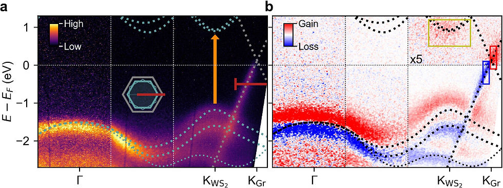
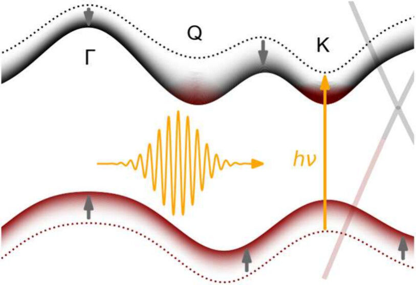
At negative pump-probe delays prior to the arrival of the pump pulse, the band structure of the WS₂-graphene sample along the ΓK-direction of the 0° WS₂ islands is presented in Figure 1a. Gray and green dashed lines are theoretical band structures for monolayer WS₂ (ref 17) and monolayer graphene (ref 18), respectively, that have been energy-shifted to match the experimentally observed doping and equilibrium gap size. The dispersion of the 30° WS₂ islands is denoted as a thin dashed green line. The orange arrow marks the electronic transition upon photoexcitation at 2 eV. Figure 1b displays the pump-induced changes in photocurrent measured at a pump-probe delay of t = 250 fs at a pump fluence of F = 1.5 mJ/cm2. Gain and loss relative to the remote unperturbed photocurrent in (Fig. 1a) are colored red and blue, respectively.
The pump-probe signal shows three prominent features:
The pump pulse populates the minimum of the WS₂ conduction band (CB) at KWS₂.
At its equilibrium position, the WS₂ VB is seen to exhibit loss, with a gain above, which shows a transient upshift.
We find that the Dirac cone associated with graphene exhibits a depletion of photoelectrons below and an enhancement of photoelectrons above the Fermi level, indicating a distribution of hot Fermi-Dirac form.
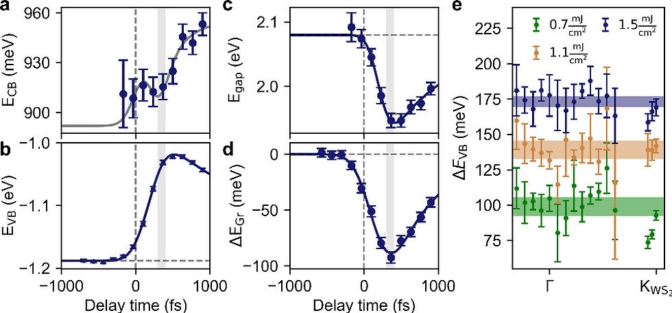
To extract the transient band gap at KWS₂ and the momentum-resolved VB shift, the researchers took as follows: they extracted energy distribution curves (EDCs) at various momenta which they fitted using a suitable number of Gaussian peaks and a Shirley background to extract the transient binding energy of the WS₂ VB and CB and the Dirac cone of graphene. The time-dependent peak position of the WS₂ conduction band (CB) and valence band (VB) at KWS₂ are present in Figures 2a and b, respectively.
Figure 2c shows the transient band gap, obtained by subtracting WS₂ VB binding energy in Figure 2b from WS₂ CB binding energy in Figure 2a, with an exponential fit. They found that the bandgap decreased by 140 ± 20 meV with a lifetime of 0.9 ± 0.2 ps in very good agreement with their own previous work and somewhat lower than what is typically found in the literature for similar samples, both experimentally and theoretically. One reason for this slight difference could be the use of another types of substrates and the difficulty of estimating the density of photoexcited electron-hole pairs in the experiment. Here, we report the transient binding energy of the Dirac cone with an exponential fit (Fig. 2d). The Dirac cone was observed to have shifted by 90 ± 10 meV with a lifetime of 0.6 ± 0.1 ps. Figure 2e shows the momentum-resolved shift of the WS₂ VB for a pump-probe delay of tmax ∼ 500 fs, when the WS₂ VB shift at KWS₂ reaches its maximum for three different fluences. The results show that within the calculated error bars the detected VB shift is momentum independent with values of 100 ± 10 meV, 140 ± 10 meV, and 170 ± 10 meV for the fluences of F = 0.7 mJ/cm^2, F = 1.0 mJ/cm^2, and F = 1.5 mJ/cm^2, respectively. This behavior is comparable to previous reports for monolayer WS₂ transferred to various substrates, showing a rigid shift, and is consistent with ab initio theory predictions for photoexcited samples.
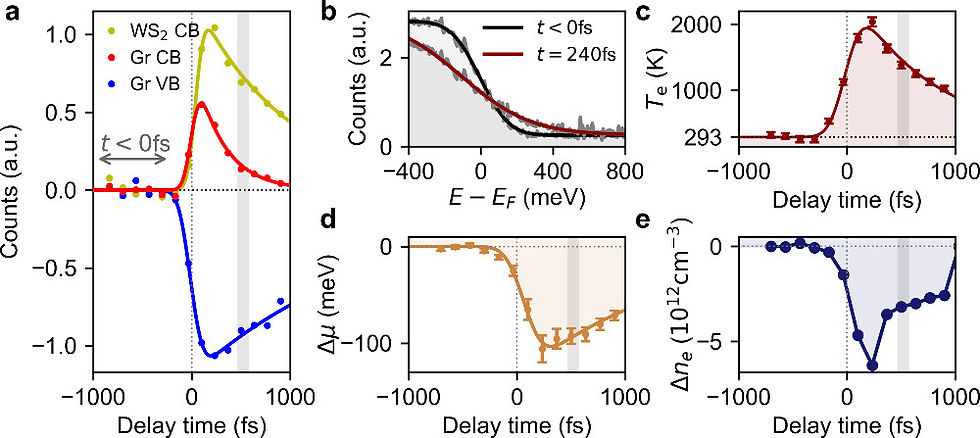
Experimentally, the researchers first found the nonequilibrium carrier distribution of the WS₂-graphene sample at the pump-probe delay responsible for the momentum-resolved WS₂ VB shift seen in Figure 2e to inform subsequent theory. Figure 3a presents the photocurrent integrated over the three areas illustrated by the colored boxes in Figure 1b as a function of pump-probe delay along with exponential fits. The Dirac cone of graphene exhibits a short-lived gain (red, τ = 300 ± 30 fs) and a long-lived loss (blue, τ = 2.10 ± 0.03 ps). The lifetime of electrons in the WS₂ CB bottom (yellow) was measured to be τ = 950 ± 70 fs. Figure 3b presents the energy-resolved population of the Dirac cone, obtained by integrating the photocurrent over the momentum range of Figure 1a marked by the red scale bar, at two distinct time delays along with respective Fermi-Dirac fits. The resultant electronic temperature(Te) and chemical potential(µ) are shown in Figs. 3c and d, respectively.
The electronic temperature peaks at Te,max = 1900 ± 100 K and decays with an exponential lifetime τ = 760 ± 60 fs. The researchers then derived the carrier concentration within the Dirac cone, based on the electronic temperature and the chemical potential. The response as a function of pump-probe delay is plotted in panel e of figure 3. Within the Dirac cone, the carrier concentration was found to drop transiently by (5.7 ± 1.2) × 10^12 cm^-2.
The insights from Figs 2 and 3 have already been ascribed to ultrafast charge separation in WS₂-graphene heterostructures. Excitation near the WS₂ A-exciton resonance followed by fast hole transfer into the graphene layer leads to a sub-1 ps charge-separated state. At the pump-probe delay t ∼ 500 fs when the VB shift at KWS₂ reaches its maximum, they obtained for a WS₂-graphene sample the following carrier distribution: ∼3.4 × 10^12 cm^-2 holes are transferred from WS₂ to graphene, but ∼70% of the photoexcited electrons remain in the WS₂ layer. Inside the Dirac cone, the electrons have an effective electronic temperature, Te ∼ 1400 K. The values are collected from all fluences analyzed in this work, and listed in the Table 1.
In that table, the authors reported their estimates of the total density of photogenerated electron-hole pairs at the three pump fluences used in the experiment. This value is hard to be estimated since the absorption of 2D TMDs is highly nonlinear, leading to Pauli blocking and many-body effects. For hBN-encapsulated WS₂, the predicted value for the fluences reached 0.5 mJ/cm^2, and more than <0.5 × 10^14 cm^-2 [ref 14]. A lower limit for is provided by the maximum number of holes which is observed to be transferred into the graphene layer during ultrafast charge separation.
In the parameter details in Tables 1 and 2, we are now in the position to input these values in ab initio calculations for the transient band gap renormalization and for the WS₂ VB shift. The graphene layer was hole-doped at equilibrium with the Fermi level −300 meV below the Dirac point (refer to Figure 1a), equating to a hole concentration of 7 × 10^12 cm−2. To address this, the researchers first utilized an accompanying static GdW correction on freestanding monolayer WS₂ to correct the band structure, as the screening from the graphene/SiC substrate diminishes the resulting band gap. They then calculated the transient changes in the WS₂ band structure resulting from screening by the photoexcited electron-hole pairs. For this, they took up individual photoexcited electron and hole densities of around 1 × 10^12 cm^-2 to 7 × 10^13 cm^-2 as per present estimates given in Table 2. In addition, we assume that 90% of the photoexcited holes are transferred into the graphene layer. This gives a hole density of inside the graphene layer for a WS₂ coverage of 50% of the graphene/SiC substrate. Finally, the researchers determined that (also see Table 1) all carriers have one common electronic temperature regardless of when they are carriers (electron or hole) and where they are (WS₂ or graphene) -- in the range T=1000 K - T=1400 K.
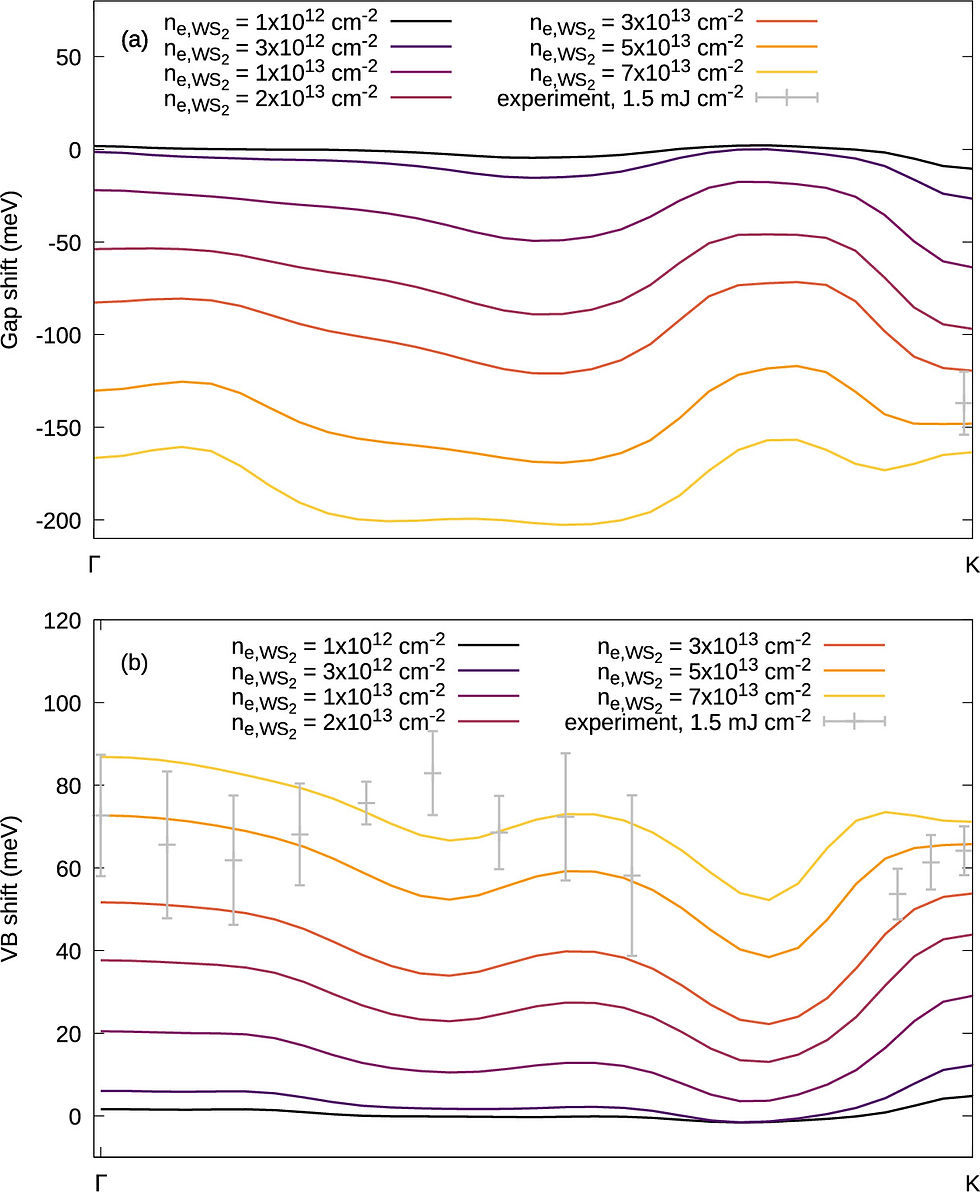
Results for the size of the transient momentum resolved gap and the VB shift at T=1500 K as a function of temporal shift are shown in Figs 4a and b, respectively. The direct WS₂ band gap at KWS₂ decreased by 11 meV (163 meV) at an electron density of 1 × 10^12 cm^-2 (7 × 10^13 cm^-2) with a k-dependent variation of 13 meV (46 meV) (Gale), produced by the presence of the adjacent graphene monolayer and the difference in Fermi levels between the WS₂ and graphene layers. The VB shift was observed to range from mean values of ∼2 meV (black) to ∼70 meV (red) for σ values present at electron densities from 1 × 1012 cm−2 to 7 × 1013 cm−2 with a k−dependent variation between ∼6 meV (black) and ∼36 meV (red). The results for T=1000 K are shown in the SI in SFigure 7.
The researchers emphasized that renormalizations due to holes in the WS₂ monolayer itself dominate over those caused by holes in the relatively remote graphene layer (SFigure 11). Based on their work, the researchers stated, "We demonstrated that WS₂ on graphene presents a massive light-induced renormalization of the band structure, which is well described by our ab initio theory that includes Hartree and GW contributions of WS₂ and GdW contributions of the graphene substrate. The experimental error bars, though, are too large to permit checking experimentally the theoretically predicted k-dependence of the transient band structure changes. The atomic-level details revealed in this work should, therefore, aid the design of future optoelectronic devices that incorporate monolayer TMDs and their heterostructures with graphene."
These findings are likely to play an important role in future technological and industrial developments, including cutting-edge optoelectronic devices. Reference k-Resolved Ultrafast Light-Induced Band Renormalization in Monolayer WS₂ on Graphene
Niklas Hofmann, Alexander Steinhoff, Razvan Krause, Neeraj Mishra, Giorgio Orlandini, Stiven Forti, Camilla Coletti, Tim O. Wehling, Isabella Gierz https://pubs.acs.org/doi/10.1021/acs.nanolett.4c06238 Nanotechnology World (NW)


Comments