Physicists explain metallic conductivity of thin carbon nanotube films
- Marine Le Bouar
- Nov 22, 2017
- 4 min read

An international team of researchers from MIPT; Lebedev Physical Institute, RAS; Prokhorov General Physics Institute, RAS; Skoltech; and Aalto University (Finland) has examined the optical and dielectric properties of thin macroscopic films based on single-walled carbon nanotubes and obtained an explanation for the metallic nature of their conductivity using infrared and terahertz spectroscopy. The research findings were published in the journals Carbon and Nanotechnology.
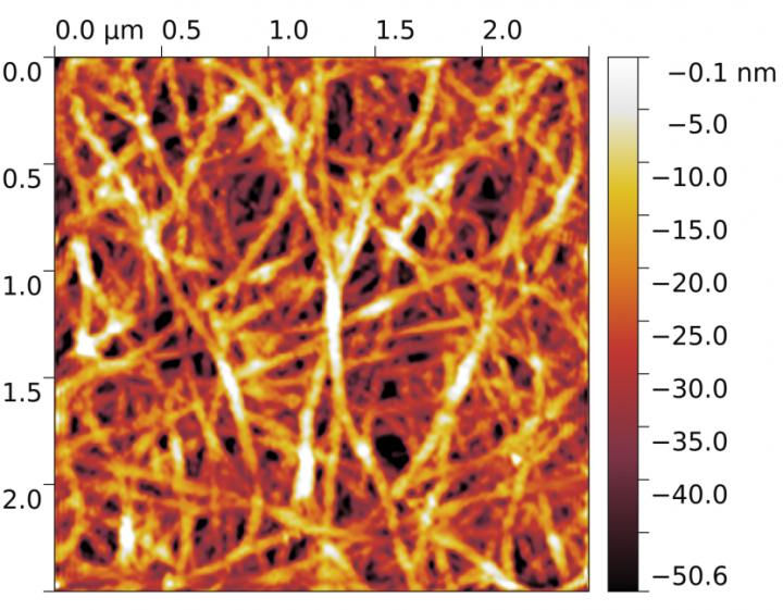
A single-walled carbon nanotube, or SWNT, can be pictured as a graphene sheet rolled into a cylinder. Light, strong, and resistant to high temperatures, SWNTs can be used as additives to composite materials to make them more durable, or as building blocks to fabricate aerosol filters and electrochemical sensors. Transparent and flexible carbon nanotube films -- that is, 2-D structures formed by intersecting nanotubes -- have a wide variety of potential applications, for example as supercapacitors or transparent electrodes in flexible electronics -- electronic devices that can be bent, folded, and twisted without breaking. The study of the charge transfer mechanisms in such films is therefore important for both basic research and practical applications.
The physicists measured optical and electrical properties of the films by terahertz-infrared spectroscopy at a variety of temperatures, from -268 degrees Celsius to room temperature, and in a wide range of incident radiation wavelengths -- from ultraviolet to terahertz (wavelengths of about 1 millimeter). The study of the interaction between the films and radiation yielded fundamental data on the electrodynamics of the films.
The SWNT films were synthesized by using aerosol chemical vapor deposition (CVD). Briefly, a vapor of the catalyst precursor ferrocene is supplied into the CVD reactor, where it decomposes in the atmosphere of carbon monoxide, forming nanometer-sized catalyst particles. On their surface, carbon monoxide (CO) disproportionation -- simultaneous oxidation and reduction -- occurs and finally SWNTs grow. The flow at the outlet of the rector is filtered, and SWNTs are collected onto the nitrocellulose filter. By varying the duration of the collection time, one could obtain the films of different thicknesses. Importantly, the SWNT films can be easily transferred to different substrates by dry deposition or used in their free-standing form, that is, without a substrate. This method enables the production of high-quality nanotubes with no amorphous carbon impurities.

"Since all carbon atoms in SWNTs are located on their surface, it is relatively easy to alter the electrical properties of this unique material. We can improve the conductivity of the films either by incorporating dopants into the nanotubes or by coating them with electron-acceptor or -donor molecules," comments Professor Albert Nasibulin of Skoltech. In their studies, the scientists coated the samples with gold chloride, whose solution acted as a doping agent, and obtained films from nanotubes filled with iodine and copper chloride by placing them in the atmosphere of the appropriate vapors. Such treatment increases charge carrier density in the filled tubes and reduces contact resistance between them, enabling flexible transparent electrodes and materials with selective charge transfer for use in optoelectronics and spintronics.
To be used in electronics, films need to be efficient charge carriers, so the physicists examined the broadband spectrum of their dielectric permittivity. But flexible electronics will also require the films to be transparent, so their optical conductivity was measured as well. Both analyses were conducted in a wide temperature range, from several degrees above absolute zero to room temperature. Of particular interest are the data obtained in the terahertz and far infrared regions of the spectrum. While prior research findings pointed to a peak in the terahertz conductivity spectrum (at frequencies between about 0.4 and 30 THz, depending on the study), this paper reports no clear indications of the phenomenon. The authors attribute such results to the high quality of their films.
Since the analysis of the optical and dielectric properties of the films at frequencies below 1,000 cm?¹ revealed spectral features that were typical for conducting materials, like metals, the team decided to employ the corresponding conductivity model that was developed by Paul Drude.
According to that model, the charge in the conductors is transferred by free carriers: Like the ideal gas molecules, they move between the ions in the lattice and scatter upon collision with its vibrations, defects, or impurities. In this study, the charge carriers are also scattered by the energy barriers at the intersections of individual nanotubes. However, as the analysis suggests, these barriers are insignificant and allow the electrons to move almost freely across the film. Using the Drude model, the authors were able to quantitatively analyze the temperature dependencies of the carriers' effective parameters -- namely, concentration, mobility, mean free path and time between collisions -- which are responsible for the electrodynamic properties of the films.
"Our research has clearly demonstrated that terahertz spectroscopy provides an efficient tool for studying the conductivity mechanisms in macro-scale carbon nanotube films and determining the effective parameters of charge carriers in a noncontact manner. Our findings show that such films may be successfully used as components or assemblies in various micro- and nanoelectronic devices," says Elena Zhukova, deputy head of the Laboratory of Terahertz Spectroscopy at MIPT.
Terahertz spectroscopy of charge transport in films of pristine and doped single-wall carbon nanotubes B.P. Gorshunov, E.S. Zhukova, Ju.S. Starovatykh, M.A.Belyanchikov, A.K.Grebenko, A.V.Bubis, V.I.Tsebro, A.A.Tonkikh, D.V.Rybkovskiy, A.G.Nasibulin, E.I.Kauppinen, E.D.Obraztsova https://doi.org/10.1016/j.carbon.2017.10.072


