Nanotube letters spell progress
- Marine Le Bouar
- Dec 7, 2015
- 4 min read
Never mind the ABCs. Rice University scientists interested in nanotubes are studying their XYΩs.
Carbon nanotubes grown in a furnace aren’t always straight. Sometimes they curve and kink, and sometimes they branch off in several directions. The Rice researchers realized they now had the tools available to examine just how tough those branches are.
They used experiments and simulations to study the stiffness of joined nanotubes and found significant differences that are defined by their forms. It turned out that some types are tougher than others, and that all may have their uses if and when nanotubes are used to build macroscale structures.
The team led by Rice materials scientist Pulickel Ajayan and theoretical physicist Boris Yakobson named their nanotubes for their shapes: I for straight nanotubes, Y for branched, X for covalently joined tubes that cross, the lambda symbol (an upside-down “V”) for nanotubes that join at any angle and the omega symbol (Ω) for noncovalent tubes that bind through van der Waals and other forces.
They said targeted synthesis of this “nanotube alphabet” may provide material for future nanoscale structures with tunable mechanisms.
The study was published by the American Chemical Society’s Nano Letters.
“We needed some sort of language to describe the specific configuration of the junctions, so we thought, ‘Let’s use letters,’” said Evgeni Penev, a co-author and research scientist in Yakobson’s group.
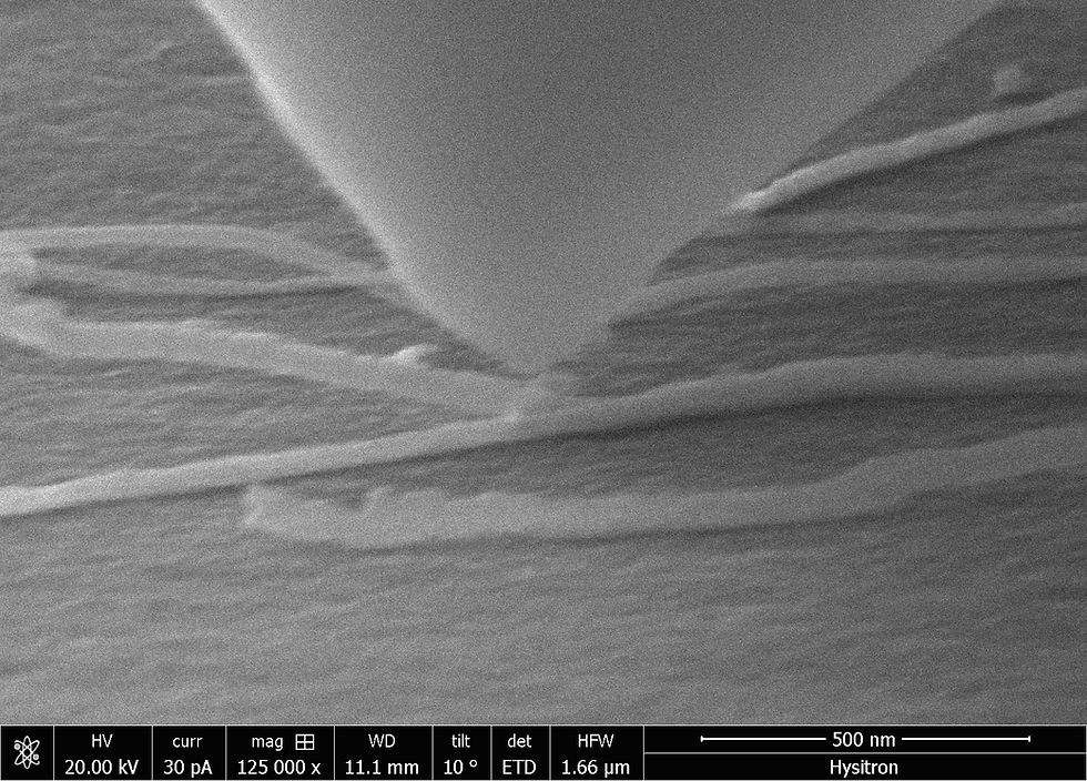
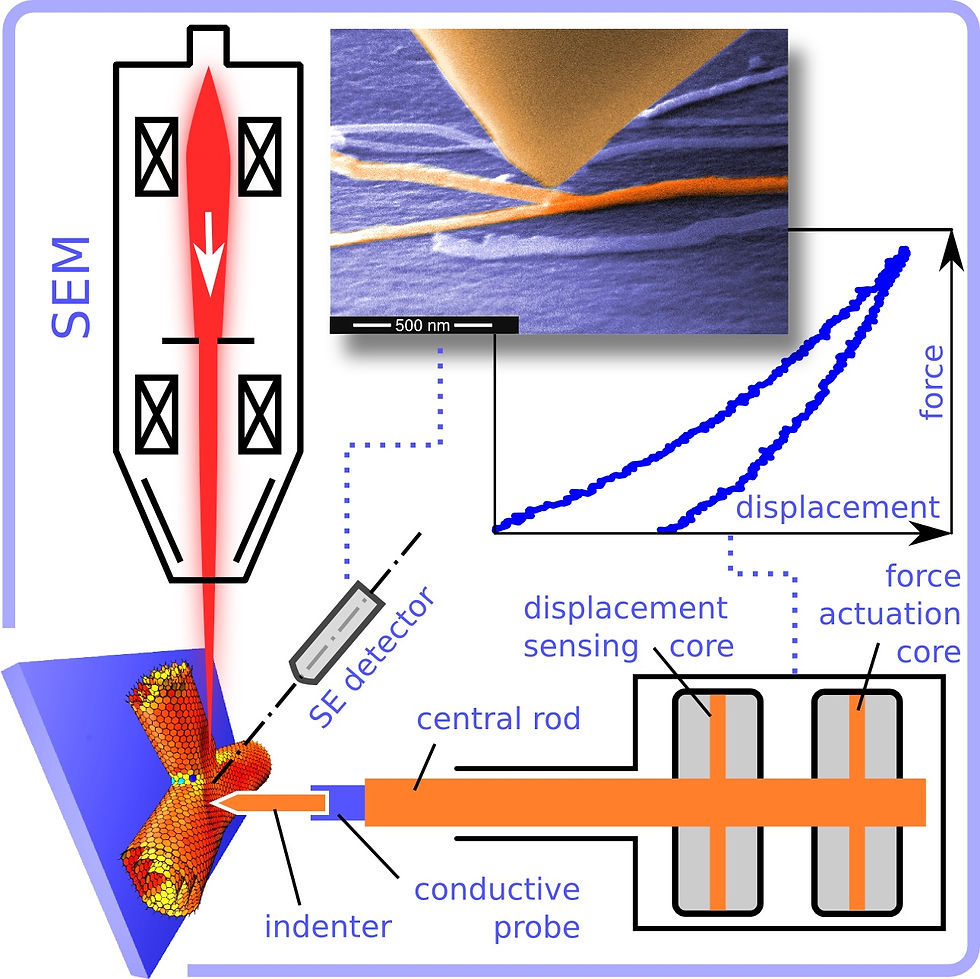
Chandra Sekhar Tiwary, a postdoctoral researcher in the Ajayan lab, prodded the nanotube junctions with a PicoIndenter that measures force and displacement in nanonewtons (billionths of a newton, a unit of force) and nanometers. The PicoIndenter was installed on a scanning electron microscope at Hysitron, a nanomechanical test-instruments manufacturing and testing company in Minneapolis.
Nanotubes grown by Rice graduate student Sehmus Ozden were dispersed in a solution, dried on silicon and placed under the microscope, where Tiwary scanned them for candidate “letters.” He then had to be sure those candidates were single units and not just two separate nanotubes. “The space between the tubes could be as little as 1 nanometer but the resolution of the microscope was 5 nanometers, so we had to pick up one side (of the nanotubes) to be sure they were truly welded,” he said. “If the nanotubes separated easily, we moved on to the next candidate.”
Applying the probe to a particular spot on an individual nanotube was a test of patience, Tiwary said. Once a good candidate appeared, he and Hysitron senior staff scientist and co-author Sanjit Bhowmick zeroed in on the junction and, over 20 minutes, slowly applied and released enough pressure to compress it without breaking it. “In the old days, these tests used brute force, but the new tools are remarkable,” Tiwary said. “We were able to watch as we compressed the nanotubes.”

Among the atomically bonded tubes, they found the X’s were the stiffest and most able to bounce back to nearly their original shapes. Next came Y’s and then the any-angle lambdas, but all were left with dents because of newly created links between the inner walls. The I’s and omegas, with no covalent bonds joining them to other nanotubes, returned to their original configurations.
The experimentalists turned to graduate student Yang Yang of Yakobson’s theoretical group to help understand the mechanism by which the nanotubes handled stress. Yang created atom-level, triple-walled computer models of each “letter” and tested their strength with virtual probes.
“In experiments, we get what is happening quantitatively, but they cannot tell us what is happening inside the tubes,” Tiwary said. “Until they did the calculations, we didn’t really know how carbon nanotube junctions behaved.”
The answer had to do with the atomic geometry at the junctions. Where nanotubes join, carbon atoms that normally come together in six-member rings are often forced to change their configurations, adjusting to five- and seven-member rings (known as dislocations) to remain in the lowest-energy state.
The number of dislocations required to make a nanotube branch is different for each angle. Because the dislocations take the brunt of the force, those variations determine the overall stiffness of the nanotube letter, they determined.

Previous research by Yakobson’s group found that while graphene, the atom-thick, chicken-wire-like form of carbon, is extraordinarily strong, it does not stretch very well. But the new simulations also showed the local walls of the nanotubes (which are basically rolled-up graphene) stretch enough to distribute strain applied to the junctions.
Penev suggested that nanotube carpets of certain letters could have material benefits. “Imagine if all the nanotubes were upside-down ‘Y’ shapes,” he said. “Such a carpet would be much harder to crush under pressure.”
One question now is whether scientists can grow homogenous batches of letters. “Can we have all Y’s and align them perfectly? Or can we have all X interconnects and then make a structure?” Tiwary asked. “That is going to be the next challenge, but it’s just a matter of people putting time into it. I’m optimistic.”

Syed Asif, director of research and development at Hysitron, is a co-author of the paper. Yakobson is the Karl F. Hasselmann Professor of Materials Science and NanoEngineering and a professor of chemistry. Ajayan is chair of Rice’s Department of Materials Science and NanoEngineering, the Benjamin M. and Mary Greenwood Anderson Professor in Engineering and a professor of chemistry.
The research was supported by the U.S. Department of Defense Air Force Office of Scientific Research for the Project MURI: “Synthesis and Characterization of 3-D Carbon Nanotube Solid Networks.” Computer resources were provided by XSEDE and Rice’s DAVinCI cluster, both supported by the National Science Foundation.


